


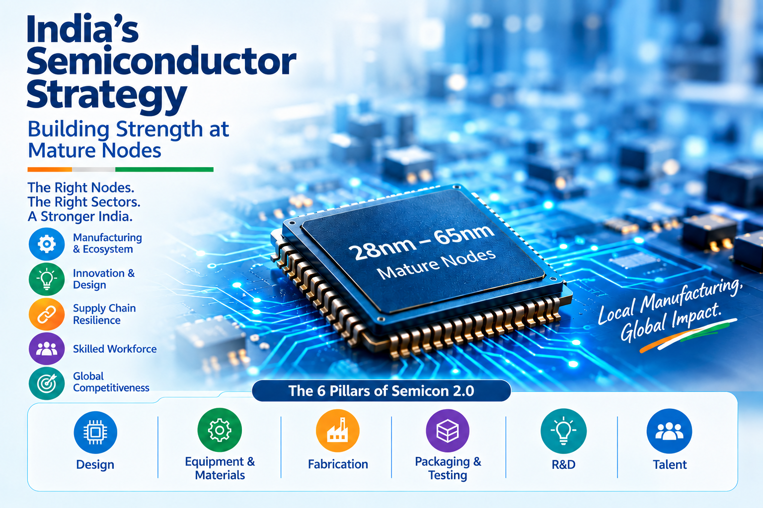
India’s Semiconductor Strategy: Building Strength at Mature Nodes
India isn’t racing Taiwan, South Korea and the United States to the bleeding edge of chip manufacturing — and that’s precisely the point. As the country works to establish itself as a dependable link in the global semiconductor supply chain, its opening move has been deliberate: focus on mature and established process nodes, particularly the 28nm–65nm range, which power the industries that never go out of demand — automotive, telecommunications, industrial electronics, power electronics and consumer appliances.
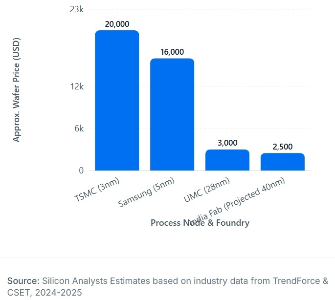
The logic here is pure semiconductor economics. Leading-edge fabs demand staggering capital outlay, deep research capability and supplier ecosystems built over decades. Mature-node manufacturing plays by different rules — reliability, cost and supply security matter more than shaving nanometres off transistor size. For India, that difference is an opening: build real manufacturing muscle now, while growing the wider ecosystem a semiconductor industry actually needs to survive long-term.
India’s Strategic Play: “More than Moore”
Think of India’s approach through the lens of “More than Moore” — a strategy built on functional diversification rather than a single-minded chase for smaller transistors. Mature-node chips aren’t a stopgap; they’re the backbone of automobiles, industrial automation, telecom equipment, power management and the Internet of Things — sectors that aren’t going anywhere.
That gives India something valuable: a genuinely large domestic demand base. As local chip production scales up, it feeds directly into India’s booming electronics manufacturing sector — and that growth, in turn, generates fresh demand for more domestically made chips. It’s a reinforcing loop, not a one-way bet.
Just as importantly, this strategy lets India sidestep an immediate, capital-heavy showdown with entrenched leaders like TSMC, Samsung and Intel at the most advanced process nodes. Instead, India gets room to build real expertise — in manufacturing discipline, process engineering, supply-chain management and yield optimisation — around mature technologies first, before pushing toward more advanced ones.
From Semicon 1.0 to Semicon 2.0
None of this is theoretical anymore. The Semicon India Programme has already laid real foundations. The original scheme, backed by a ₹76,000 crore outlay, set out to build a domestic semiconductor and display manufacturing ecosystem from the ground up. Three facilities — Micron, Kaynes Semicon and CG Power — have already moved from blueprint to commercial production.
Semicon 2.0 takes that momentum further. Approved by the Union Cabinet in July 2026 with a ₹1,27,500 crore outlay, the programme rests on six pillars: chip design, semiconductor machines and materials, fabrication, advanced packaging, research and development, and talent development.
Crucially, Semicon 2.0 isn’t a pivot away from the mature-node approach — it’s a continuation of it. The government has been explicit that India’s semiconductor journey began at 28nm–110nm nodes, with the next phase aimed at pushing into more advanced technologies. Read together, this is a phased climb, not a leap: build manufacturing competence and ecosystem depth at mature nodes first, then use that base to move up the technology ladder.
Why Mature Nodes Remain Important Under Semicon 2.0
It would be a mistake to read Semicon 2.0’s push toward advanced technology as a sign that mature nodes are yesterday’s strategy. If anything, the programme’s broader ecosystem thinking could make India’s mature-node position even stronger.
Take the programme’s emphasis on domestic semiconductor equipment, materials, chemicals and industrial gases — an unglamorous but essential piece of the puzzle. A semiconductor industry doesn’t become competitive just by building fabs; it needs a deep bench of suppliers who can deliver critical inputs and services reliably. Localising these capabilities cuts import dependence, strengthens supply-chain resilience, and opens the door for Indian companies and MSMEs to plug into global semiconductor value chains.
The same logic applies to ATMP/OSAT capabilities. This is where India can capture value that goes beyond simply fabricating wafers. With three facilities already in commercial production and more in the pipeline, packaging and testing are shaping up to be a genuine pillar of India’s semiconductor story — and Semicon 2.0 explicitly calls for strengthening this space further, including bringing in advanced packaging technologies.
Competitive Landscape and Geopolitical Advantage
Make no mistake — India is stepping into a crowded mature-node foundry market, one that already includes established players like GlobalFoundries, UMC and SMIC. Nobody should expect India’s edge to come from out-innovating them on process technology alone.
Instead, India’s advantage lies elsewhere — in market proximity, a formidable electronics manufacturing base, a fast-growing domestic market, and geopolitical positioning that few competitors can match. As global companies look to diversify their semiconductor supply chains away from a handful of concentrated hubs, India’s scale and comparatively stable business environment make it a compelling alternative.
The real goal, then, isn’t simply “manufacture chips in India.” It’s building an ecosystem where design, fabrication, packaging, equipment, materials and downstream electronics manufacturing all reinforce each other — each piece making the next one stronger.
Success So Far
The numbers tell their own story. India’s semiconductor programme has moved decisively from policy paper to production floor. Over five years, 12 manufacturing projects have been approved, representing more than ₹1.64 lakh crore in committed investment. Three facilities are already in commercial production, with construction underway on the rest.
But the real significance isn’t just in the fab count or the rupee figures — it’s what they represent: the initial industrial foundations of India’s semiconductor sector, spanning fabrication, assembly, testing, packaging, design and the supporting infrastructure that ties it all together.
The Road Ahead
India’s semiconductor roadmap is best understood as a phased climb, not a sprint to the smallest process node. Mature-node manufacturing provides the immediate commercial foundation — especially in sectors where established process technologies remain not just relevant, but essential. At the same time, Semicon 2.0 is building the institutional and financial scaffolding India will need to develop more advanced technologies over time.
The real test now is turning individual projects into a genuine ecosystem. Greater domestic sourcing of equipment and materials, tighter integration with electronics manufacturers, stronger packaging capabilities, a skilled workforce, and steady gains in yield and process technology — these will determine whether India’s early investments compound into lasting competitiveness.
The strategic opportunity for India, then, isn’t to replicate Taiwan’s or South Korea’s playbook overnight. It’s to build a differentiated semiconductor ecosystem — one that starts with mature nodes, captures value across the wider supply chain, and steadily climbs toward more advanced technologies.

Electronics and Computer Software Export Promotion Council of India (ESC), one of India’s most dynamic premier trade promotion organisations sponsored by the Government of India.
Copyright @ Electronics and Computer Software Export Promotion Council
